- 您现在的位置:买卖IC网 > Sheet目录983 > HI5662EVAL2 (Intersil)EVALUATION PLATFORM HI5662
�� �
�
�Application� Note� 9823�
�Evaluation� Board� Layout� and� Power�
�Supplies�
�The� HI5662� evaluation� board� is� a� four� layer� board� with� a�
�layout� optimized� for� the� best� performance� of� the� ADC.�
�Included� in� the� application� note� are� electrical� schematics� of�
�the� evaluation� board,� a� component� parts� list,� a� component�
�placement� layout� drawing� and� reproductions� of� the� various�
�board� layers� used� in� the� board� stack-up.� The� user� should�
�feel� free� to� copy� the� layout� in� their� application.� Refer� to� the�
�component� layout� and� the� evaluation� board� electrical�
�schematic� for� the� following� discussions.�
�The� HI5662� monolithic� A/D� converter� has� been� designed�
�with� separate� analog� and� digital� supply� and� ground� pins� to�
�keep� digital� noise� out� of� the� analog� signal� path.� The�
�evaluation� board� provides� separate� low� impedance� analog�
�and� digital� ground� planes� on� layer� 2.� Since� the� analog� and�
�digital� ground� planes� are� connected� together� at� a� single�
�point� where� the� power� supplies� enter� the� board,� DO� NOT� tie�
�them� together� back� at� the� power� supplies.�
�The� analog� and� digital� power� planes� are� also� kept� separate�
�on� the� evaluation� board� and� should� be� driven� by� clean� linear�
�regulated� supplies.� The� external� power� supplies� are� hooked�
�up� with� the� twisted� pair� wires� soldered� to� the� plated� through�
�holes� marked� +5VAIN,� +5VAIN1,� -5VAIN,� +5VDIN,�
�+5VD1IN,� +5VD2IN,� AGND� and� DGND.� The� +5VDIN,�
�+5VD1IN� and� +5VD2IN� are� digital� supplies� and� are� returned�
�to� DGND.� The� +5VAIN,� +5VAIN1� and� -5VAIN� are� the� analog�
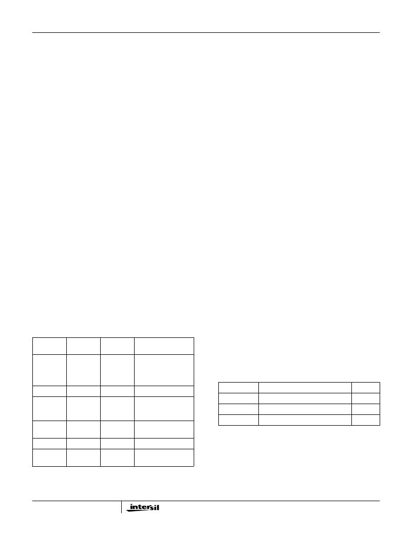
�supplies� and� are� returned� to� AGND.� Table� 1� lists� the�
�operational� supply� voltages,� typical� current� consumption� and�
�the� evaluation� board� circuit� function� being� powered.� Single�
�supply� operation� of� the� converter� is� possible� but� the� overall�
�performance� of� the� converter� may� degrade.�
�TABLE� 1.� HI5662EVAL2� EVALUATION� BOARD� POWER�
�SUPPLIES�
�Sample� Clock� Driver,� Timing� and� I/O�
�In� order� to� ensure� rated� performance� of� the� HI5662,� the� duty�
�cycle� of� the� sample� clock� should� be� held� at� 50%� ±� 5%.� It� must�
�also� have� low� phase� noise� and� operate� at� standard� TTL� levels.�
�A� CMOS� inverter� (U7)� used� as� a� voltage� comparator� is�
�provided� on� the� evaluation� board� to� generate� the� sampling�
�clock� for� the� HI5662� when� a� sinewave� (<� 2V� P-P� )� or�
�squarewave� clock� is� applied� to� the� CLK� input� (J3)� of� the�
�evaluation� board.� A� potentiometer� (VR2)� is� provided� to� allow�
�the� user� to� adjust� the� duty� cycle� of� the� sampling� clock� to�
�obtain� the� best� performance� from� the� ADC� and� to� allow� the�
�user� to� investigate� the� effects� of� expected� duty� cycle�
�variations� on� the� performance� of� the� converter.� The� HI5662�
�clock� input� trigger� level� is� approximately� 1.5V.� Therefore,� the�
�duty� cycle� of� the� sampling� clock� should� be� measured� at� this�
�1.5V� trigger� level.� U7-2� provides� a� convenient� point� to�
�monitor� the� sample� clock� duty� cycle� and� make� any� required�
�adjustments.�
�Figure� 1� shows� the� sample� clock� and� digital� data� timing�
�relationship� for� the� evaluation� board.� The� data�
�corresponding� to� a� particular� sample� will� be� available� at� the�
�digital� data� outputs� of� the� HI5662� after� the� data� latency� time,�
�t� LAT� ,� of� 6� sample� clock� cycles� plus� the� HI5662� digital� data�
�output� delay,� t� OD� .� Table� 2� lists� the� values� that� can� be�
�expected� for� the� indicated� timing� delays.� Refer� to� the� HI5662�
�data� sheet� for� additional� timing� information.�
�The� sample� clock� and� digital� output� data� signals� are� made�
�available� through� two� connectors� contained� on� the�
�evaluation� board.� The� line� buffering� provided� by� the� data�
�output� latches� allows� for� driving� long� leads� or� analyzer�
�inputs.� These� data� latches� are� not� necessary� for� the� digital�
�output� data� if� the� load� presented� to� the� converter� does� not�
�exceed� the� data� sheet� load� limits� of� 100mA� and� 15pF.� The�
�P2� I/O� connector� allows� the� evaluation� board� to� be�
�interfaced� to� the� DSP� evaluation� boards� available� from�
�POWER�
�SUPPLY�
�+5VAIN�
�NOMINAL�
�VALUE�
�5.0V� ±� 5%�
�CURRENT�
�(TYP)�
�51mA�
�FUNCTION(S)�
�SUPPLIED�
�Analog� Input� Op� Amps,�
�Reference� Voltage� Op�
�Intersil.� Alternatively,� the� digital� output� data� and� sample�
�clock� can� also� be� accessed� by� clipping� the� test� leads� of� a�
�logic� analyzer� or� data� acquisition� system� onto� the� I/O� pins� of�
�connector� header� P1.�
�Amps,� Bandgap�
�Reference�
�TABLE� 2.� TIMING� SPECIFICATIONS�
�+5VA1IN�
�-5VAIN�
�+5VDIN�
�5.0V� ±� 5%�
�-5.0V� ±� 5%�
�5.0V� ±� 5%�
�73mA�
�50mA�
�15mA�
�A/D� AV� CC1� and� AV� CC2�
�Analog� Input� Op� Amps,�
�Reference� Voltage� Op�
�Amps�
�Sample� Clock�
�PARAMETER�
�t� OD�
�t� PD1�
�t� PD2�
�DESCRIPTION�
�HI5662� Digital� Output� Data� Delay�
�U7� Prop� Delay�
�U10/11� Prop� Delay�
�TYP�
�11ns�
�9ns�
�4.5ns�
�+5VD1IN�
�+5VD2IN�
�5.0V� ±� 5%�
�5.0V� ±� 5%� or�
�3.0V� ±� 10%�
�61mA�
�4.5mA�
�Generator� and� D-FF’s�
�A/D� DV� CC1� and� DV� CC2�
�A/D� DV� CC3�
�HI5662� Performance� Characterization�
�Dynamic� testing� is� used� to� evaluate� the� performance� of� the�
�HI5662� A/D� converter.� Among� the� tests� performed� are�
�Signal-to-Noise� and� Distortion� Ratio� (SINAD),� Signal-to-�
�Noise� Ratio� (SNR),� Total� Harmonic� Distortion� (THD),�
�Spurious� Free� Dynamic� Range� (SFDR)� and� Intermodulation�
�Distortion� (IMD).�
�3-2�
�发布紧急采购,3分钟左右您将得到回复。
相关PDF资料
HI5714EVAL
EVALUATION PLATFORM HI5714
HI5728EVAL1
EVALUATION PLATFORM TQFPHI5728
HI5731-EVS
EVALUATION PLATFORM SOIC HI5731
HI5741-EVS
EVALUATION PLATFORM HI5741
HI5760EVAL1
EVALUATION PLATFORM SOIC HI5760
HI5762EVAL2
EVALUATION MOD FOR HI5762 AMP
HI5767EVAL1
EVALUATION PLATFORM HI5767
HI5767EVAL2
EVALUATION PLATFORM HI5767
相关代理商/技术参数
HI5662IN
制造商:未知厂家 制造商全称:未知厂家 功能描述:Converter IC
HI5667
制造商:INTERSIL 制造商全称:Intersil Corporation 功能描述:8-Bit, 60MSPS A/D Converter with Internal Voltage Reference
HI5667/6CA
制造商:Rochester Electronics LLC 功能描述:A/D, 8-BIT,60MSPS,COM TEMP,28 SSOP,TTL/CMOS (HI5767/6, 10- - Bulk
HI5667/6CB
制造商:Rochester Electronics LLC 功能描述:- Bulk
HI5667EVAL2
制造商:Rochester Electronics LLC 功能描述:- Bulk
HI5675
制造商:INTERSIL 制造商全称:Intersil Corporation 功能描述:8-Bit, 20MSPS, Flash A/D Converter
HI5675_03
制造商:INTERSIL 制造商全称:Intersil Corporation 功能描述:8-Bit, 20MSPS, Flash A/D Converter
HI5675JCB
制造商:Rochester Electronics LLC 功能描述:- Bulk